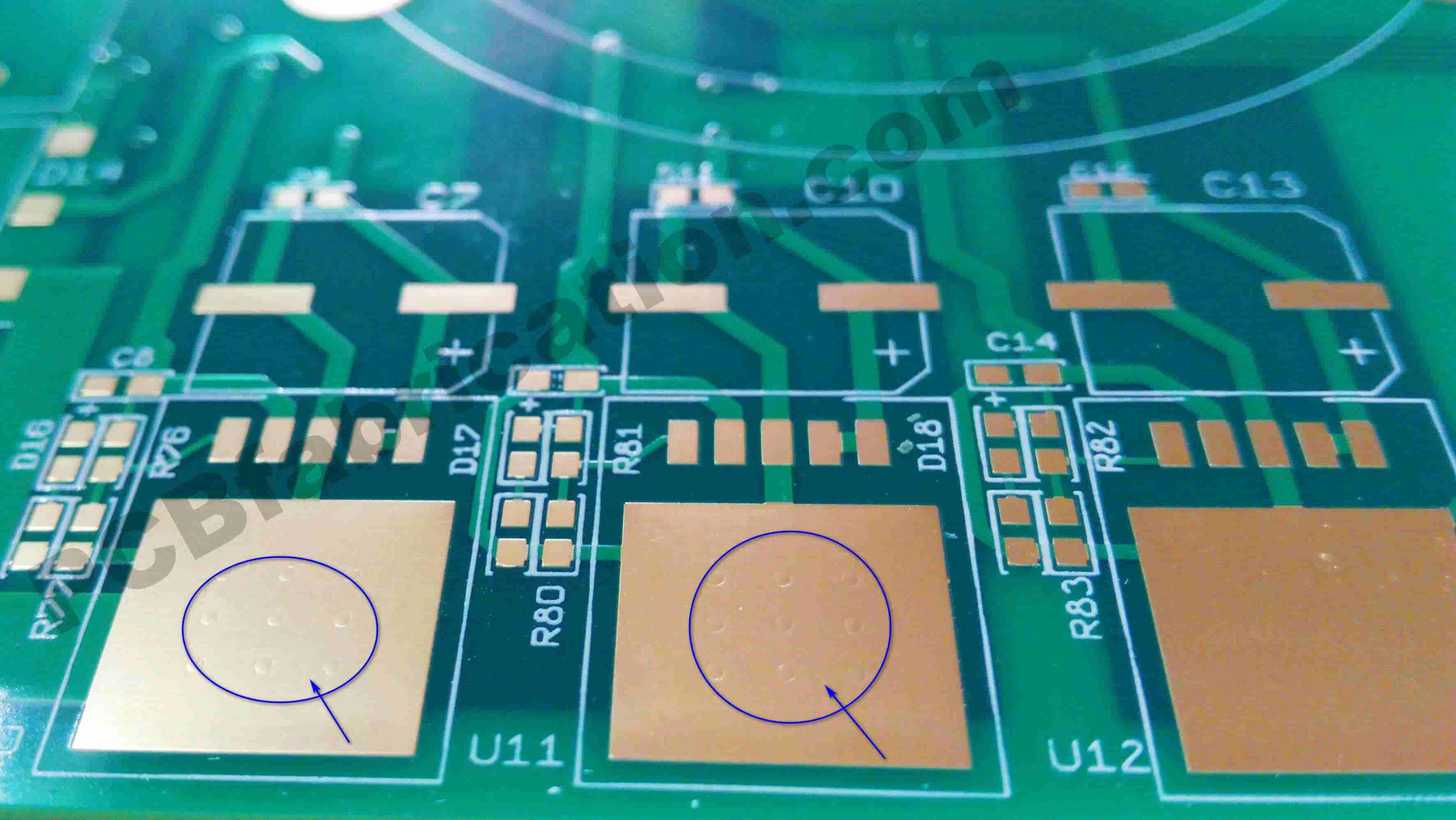
Via In Pad
- Via In Pad is a special design technology to increase PCB density, to allows higher PCB component density. Many designers like to use via in pad to significantly save board space.
- There are special processes to fabricate via in pad PCBs as it is necessary to fill the vias to have flat surface on which a CU panel plating is applied. PCB Fabrication company (www.PCBfabrication.com) can fabricate high quality single-layer, double-layer and multi-layer via in pad PCBs. But our company website can not generate automatic quote instantly online. Please email your via-in-pad PCB design files to PCB@PCBfabrication.com, my company engineers will manually quote for you.