
FAQ >> How to Design and Fabricate Blind/Buried Via Hole PCB
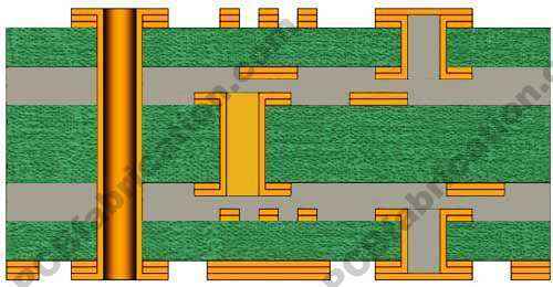
Please see the below photo about 6 layer PCB example. The green central via hole connected layer 3 to layer 4 is buried via hole. To fabricate the PCBs, first we need to make 3 sub-boards (first sub-board is for copper layer 1 and 2, second sub-board is for layer 3 and 4, and third sub-board is for 5 and 6). Finally laminate these 3 sub-boards together to get the 6 layer PCBs. So the PCBs can be fabricated if design blind via holes between layer 1 to 2, or layer 3 to 4, or layer 5 to 6. You could see there is NO way to make PCBs with vias between layer 2 and 3, or 4 and 5.
Plus the PCBs can be fabricated if design via holes between layer 1 to 4. In this case, after first sub-boards and second sub-boards are ready, we will laminate the 2 sub-boards together temporally, and then make the via holes for layer 1 to layer 4.Finally laminate 3rd sub-boards together
Plus the PCBs can be fabricated if design via holes between layer 1 to 4. In this case, after first sub-boards and second sub-boards are ready, we will laminate the 2 sub-boards together temporally, and then make the via holes for layer 1 to layer 4.Finally laminate 3rd sub-boards together