
PCB Microsectioning
PCB microsectioning is an important method used in PCB quality evaluation and process control. It helps reveal hidden internal features that cannot be checked from the board surface alone. For many high-reliability products, microsection analysis is a valuable tool for confirming plating quality, layer structure, and hole integrity.
What Is PCB Microsectioning?
Microsectioning is a process in which a selected portion of a PCB is cut, mounted, polished, and examined under magnification. It allows engineers and quality personnel to inspect internal structures such as copper plating, dielectric layers, hole wall condition, and layer-to-layer alignment.
- Used for quality assurance and process verification
- Helps detect hidden or subsurface defects
- Can confirm whether fabricated structures match design intent
- Often used for plated through holes, vias, and multilayer boards
Why Is Microsectioning Important?
| Inspection Area | Why It Matters |
|---|---|
| Plated hole wall | Helps verify copper plating quality and detect voids, cracks, or insufficient thickness. |
| Layer structure | Confirms dielectric thickness, copper thickness, and stackup consistency. |
| Interconnection reliability | Supports evaluation of vias and plated through holes in multilayer PCBs. |
| Manufacturing process control | Provides feedback for drilling, plating, lamination, and other fabrication steps. |
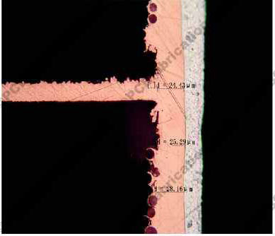
What Can Be Checked in a PCB Microsection?
- Plated copper thickness in holes
- Hole wall quality and inner layer connection
- Dielectric thickness between layers
- Copper foil thickness
- Registration between drilled holes and internal pads
- Evidence of cracks, voids, resin recession, or other internal defects

When Should Microsectioning Be Requested?
Microsectioning may be requested when a project has higher reliability requirements, special quality verification needs, or engineering validation requirements. If your PCB design includes critical vias, multilayer interconnections, or strict internal structure control, it is helpful to communicate that requirement clearly before production.