
Blind & Buried Via PCB (HDI)
Sequential lamination, copper-filled microvias, and fine-pitch HDI routing
HDI • Microvias • Stacked Vias • IPC-2226 • Impedance
HDI Overview & Benefits
- Shorter via stubs for high-speed signals
- Enables fine-pitch BGA escape routing
- Higher wiring density per layer
- Better RF & high-speed digital performance
Types of Vias (HDI)
- Blind Via: L1→L2 / L(n)→L(n-1)
- Buried Via: inner-layer to inner-layer
- Laser Microvia: copper-filled
- Stacked / Staggered Microvias
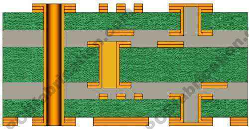
Example: buried via in HDI stack-up
HDI Design Rules
| Item | Guideline | Notes |
|---|---|---|
| Laser microvia | 0.10–0.20 mm | Filled for stacking |
| Aspect ratio | ≤ 1:1 | Reliability requirement |
| Stacked vias | 1–2 layers | More = higher cost |
| Lamination cycles | 1–2 | Sequential lamination |
| Core via | 0.20–0.30 mm | Standard drill |
Smartphones commonly use 3-layer stacked microvias
Typical HDI Stack Examples
| Layers | Type | Description |
|---|---|---|
| 6-Layer | 1-step | L1→L2, L6→L5 |
| 8-Layer | 1+N+1 | Microvia + buried core |
| 10-Layer | 2+N+2 | Stacked microvias |
Avoid vias between L2-L3 / L4-L5 in standard six-layer
HDI Manufacturing Process
- Build core
- Laser microvias
- Copper fill
- Lamination press
- Mechanical through-drill
- Electroplating
- AOI & electrical test
Send Your HDI Stackup for Review
We check lamination order, via reliability, and impedance needs.