How to Change PCB Gerber File
This step-by-step tutorial explains how to change a PCB Gerber file in Altium Designer CAM Editor. In this example, a new copper trace and a pad are added on the top layer, and the corresponding drill hole is created as well.
Before You Start
Gerber editing can be useful when a small PCB manufacturing change is needed after Gerber output has already been generated. This guide focuses on a simple example only.
- Software used in this example: Altium Designer CAM Editor
- Modification example: add a pad, a drill hole, and a copper trace
- Output result: updated Gerber files and NC Drill data
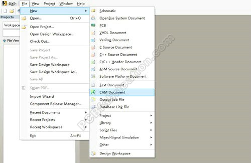
Step 1: Open Altium Designer and create a new CAM file
Start Altium Designer and create a new CAM document for PCB Gerber editing.
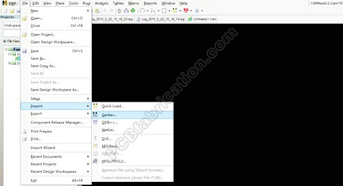
Step 2: Import the original Gerber and drill files
Import the original Gerber files and the NC drill file into the CAM Editor so the existing PCB data can be edited.
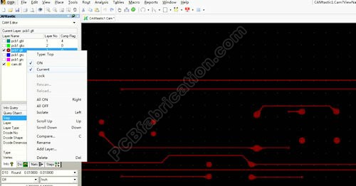
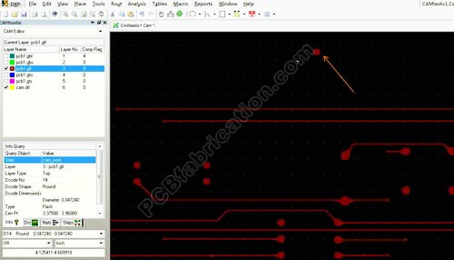
Step 3: Set the .GTL file as the current working layer
Select the .GTL (Gerber Top Layer) file as the current layer, because the new copper feature will be added to the top layer.
Step 4: Place a new pad on the top layer
From the Place menu, select Flash and put a new pad at the desired location in the PCB window.
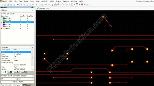
Step 5: Add a drill hole at the center of the new pad
Switch to the Drill Hole window, change the CAM Editor to the NC Editor, then use Place > Drill > Drillpoint to add a drill hole at the center of the new pad.
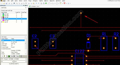
Step 6: Add a new copper trace connected to the pad
Switch back to CAM Editor, select the .GTL layer again, and use the Place menu to add a new copper line connected to the new pad.
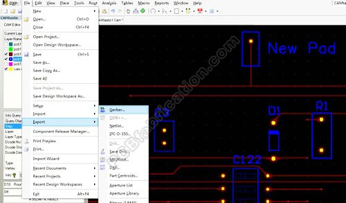
Step 7: Export the updated Gerber file for PCB fabrication
After finishing the modification, export the updated Gerber file and corresponding drill data for PCB fabrication.